Today I am going to explain a helpful technique used while designing embedded system. The technique is to expand the number of input and output lines available in any microcontroller. The idea is to use a shift register, a shift register help us load data in a serial fashion (requiring less number of i/o lines) and then convert the data into a parallel form that can drive many types of load like LED,Relays, motor etc, just like normal i/o ports of MCU. Their are two advantage of this method:-
- Only three i/o lines can drive virtually any number of output ports.
- Say if you want to control 50 leds that are at the distance of 2 meter from the controller then you save lots of wires! and mess up too!
The above described what we called an output shift register. Another type is an input shift register. This type is used to take input. It does reverse of the output shift register. It takes parallel input and transfer it serially to the MCU. The most common commercial example I found is the NES joystick. Their are 8 buttons (you will notice 10 but 2 of it are turbo, that means they repeat action A or B(turbo A or B pressed) at particular frequency when kept depressed) The designers didn’t ran 9 pins from the consol to the joystick (approx 1.5 meters). Instead they put a input shift register on the joystick and used 5 pins for data transfer. In this way they wisely saved money and increased the reliability of the joystick (thin cable, less wires and better connector). We will describe input shift register in latter tutorial. In this tutorial we will learn about the output shift register IC 74HC595, develop routines for AVR in avr-gcc, and finally test those routines using a simple example. So lets begin.
Output Shift Register 74HC595
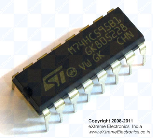 |
74HC595 IC |
The output shift register IC 74HC595 fits perfectly in our needs. A block diagram of 74HC595 is shown below.
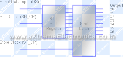 |
Block Diagram of 74HC595 IC |
As you can see in the above image their are three signal lines which connects a 74HC595 to any microcontroller. They are :-
- Serial Data Input (DS) – on this pin mcu outputs the data serially.
- Shift Clock (SH_CP) – on this pin clock signal is applied. On every rising edge the data on the DS line is sampled and it enters the shift register. The bit on DS line is stored on the LSB (least significant place i.e. BIT0). On next pulse this bit moves to BIT1 location. After 8 clock pulses this bit is moved to BIT7 (MSB place). After 8 clock pulses the Shift Register has all 8 bits of a byte and is ready to convert them to parallel. Now the ST_CP line (described next) comes to the scene.
- Store Clock (ST_CP) – On a rising edge the data stored in shift register is transferred parallel to a 8 bit latch which is connected directly to the output pins.
avr-gcc source code for 74HC595
Our 74HC595 module consist of following functions.
void HC595Init()
Initializes the shift register sub-system. The only this this function does is to set the i/o lines of the MCU that connects to 74HC595 as output.
HC595DataHigh() – Makes the data line high (1)
HC595DataLow() – Makes the data line low (0)
void HC595Pulse()
This function sends a pulse to the Shift Clock.
void HC595Latch()
This function moves the data in the shift register to the latch using a pulse on store clock line. When all bits have been transferred this function is called to make the data available on output. Until this function is called the latch contains the data that was loaded last time by pulsing the store clock signal. Remember latch is separate from the shift register so data shifting is not available on latch during shift phase. It is only made available when all 8 bits are in their required positions. This make the extended port atomic.
void HC595Write(uint8_t data)
This is the only high level function of the module. It uses the above four low level function to transmit a full byte to the extended output port. You don’t need to call any of the four low level functions directly. Just call HC595Write with any byte as parameter, the same byte will be available on the output line of HC595 IC.
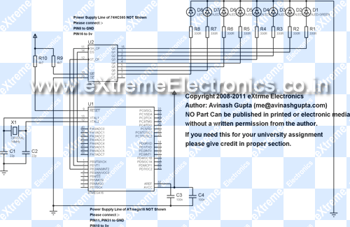
Schematic for ATmega16 interface with 74HC595
We will make a simple example where we will drive 8 leds using shift register ic 74hc595.
AVR interface with 74HC595 |
You can build the circuit using our low cost avr development board. The board has the basic circuit to sustain a MCU like ATmega16 or ATmega32. In that case you just have to build the 74HC595 part. That is the LEDs connect to 74HC595 using series resistor on a small bread board. You can then connect the 74HC595 part to the MCUs PORTB using a single pin female to female burg wires.
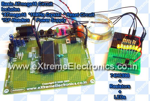 |
ATmega16 connected to 74HC595 |
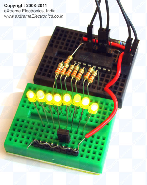 |
74HC595 with LEDs |
avr-gcc example for 8 led drive using shift register
#include <avr/io.h>
#include <util/delay.h>

/***************************************

Configure Connections

****************************************/

#define HC595_PORT   PORTB
#define HC595_DDR    DDRB

#define HC595_DS_POS PB0      //Data pin (DS) pin location

#define HC595_SH_CP_POS PB1      //Shift Clock (SH_CP) pin location
#define HC595_ST_CP_POS PB2      //Store Clock (ST_CP) pin location

/***************************************
Configure Connections ***ENDS***
****************************************/

//Initialize HC595 System

void HC595Init()
{
   //Make the Data(DS), Shift clock (SH_CP), Store Clock (ST_CP) lines output
   HC595_DDR|=((1<<HC595_SH_CP_POS)|(1<<HC595_ST_CP_POS)|(1<<HC595_DS_POS));
}


//Low level macros to change data (DS)lines
#define HC595DataHigh() (HC595_PORT|=(1<<HC595_DS_POS))

#define HC595DataLow() (HC595_PORT&=(~(1<<HC595_DS_POS)))

//Sends a clock pulse on SH_CP line
void HC595Pulse()
{
   //Pulse the Shift Clock

   HC595_PORT|=(1<<HC595_SH_CP_POS);//HIGH

   HC595_PORT&=(~(1<<HC595_SH_CP_POS));//LOW

}

//Sends a clock pulse on ST_CP line
void HC595Latch()
{
   //Pulse the Store Clock

   HC595_PORT|=(1<<HC595_ST_CP_POS);//HIGH
   _delay_loop_1(1);

   HC595_PORT&=(~(1<<HC595_ST_CP_POS));//LOW
   _delay_loop_1(1);
}


/*

Main High level function to write a single byte to
Output shift register 74HC595.

Arguments:
   single byte to write to the 74HC595 IC

Returns:
   NONE

Description:
   The byte is serially transfered to 74HC595
   and then latched. The byte is then available on
   output line Q0 to Q7 of the HC595 IC.

*/
void HC595Write(uint8_t data)
{
   //Send each 8 bits serially

   //Order is MSB first
   for(uint8_t i=0;i<8;i++)
   {
      //Output the data on DS line according to the
      //Value of MSB
      if(data & 0b10000000)
      {
         //MSB is 1 so output high

         HC595DataHigh();
      }
      else
      {
         //MSB is 0 so output high
         HC595DataLow();
      }

      HC595Pulse();  //Pulse the Clock line
      data=data<<1;  //Now bring next bit at MSB position

   }

   //Now all 8 bits have been transferred to shift register
   //Move them to output latch at one
   HC595Latch();
}

/*

Simple Delay function approx 0.5 seconds

*/

void Wait()
{
   for(uint8_t i=0;i<30;i++)
   {
      _delay_loop_2(0);
   }
}

void main()
{
   uint8_t led_pattern[8]={
                        0b10000001,
                        0b11000011,
                        0b11100111,
                        0b11111111,
                        0b01111110,
                        0b00111100,
                        0b00011000,
                        0b00000000,
                     };

   //Initialize HC595 system

   HC595Init();

   while(1)
   {
      for(uint8_t i=0;i<8;i++)
      {
         HC595Write(led_pattern[i]);   //Write the data to HC595
         Wait();                 //Wait

      }
   }


}
The code can be compiled using WinAVR Compiler using the AVR Studio as front end. For more details on installing and using this tool please see the following tutorial.
Compile the above program using AVR Studio (compiler is avr-gcc). And finally burn the program using any ISP Programmer to the ATmega16. The fuse bits must be set as following to enable external crystal as clock source.
- High Fuse = C9 (hex value)
- Low fuse =FF (hex value)
After burning the HEX file to MCU, finally you are ready to power up the setup.
Things Required
- 74HC595 Shift Register IC in DIP Package(Serial In, Parallel Out)
- Breadboard (Can be used for other projects too!)
- Male Headers 15mm
- Single pin female to female wire
- 40 PIN Low Cost AVR Development Board. (Can be used for other projects too!)
- USB AVR Programmer.(Can be used for other projects too!)
- Resistors, LEDs etc.
Help Us!
We try to publish beginner friendly tutorials for latest subjects in embedded system as fast as we can. If you like these tutorials and they have helped you solve problems, please help us in return. You can donate any amount as you like securely using a Credit or Debit Card or Paypal.
We would be very thankful for your kind help.
Downloads
Video for Shift Register 74HC595
Subscribe!
Don’t miss any article get them right in your inbox! Subscribe to our feeds powered by Feedburner.
By
Avinash Gupta
www.AvinashGupta.com
me@avinashgupta.com
Facing problem with your embedded, electronics or robotics project? We are here to help!
Post a help request.



Its the most awaited post for me.. Thankyou sir very much..
again a nice,helpful tutorial sir. now i dnt have to solder so many wires..it solved my problem :)thanku and keep going
Every time you provide some unique and useful thing, that is the beauty of your site. Thank you.
Can you please provide some practical/useful application of this serial to parallel bit transfer application which can be realized in hobby/home level
Regards,
Uttam
Awesome article……..was really looking for it.
@Uttam Dutta: You can use these registers to build a moving message display or something like that.
Thank You Ramanpreet, Can you provide any such schematic
Regards,
Uttam
why didnt u use spi for this ?? u cud use these with spi without ne problems
ne ways good work
Thanks for sharing.
I want to do output extension with internal oscillator is it ok or externel 16MHz is required?
——————
“People rarely succeed unless they have fun in what they are doing”.
Hello,
i tested your programm on my ATmega16 but after half of the time the LEDs are blinking anyway.
Here is a video i have made.
http://www.youtube.com/watch?v=xc3FV-h1sUs&feature=youtu.be
do you know what´s the problem?
really helped me.. 🙂
very helpful tutorial
sir one request to you.please release PDF version of tutorial
your tutorials are awesome….. i have learned so much from you 🙂 thanks a lot 🙂 🙂 🙂
Thanks for this but I would like to connect the out put of 74hc595 to 16×2 LCD ,can you help in this regard and the changes to the code pleas?
Dear all,
Im using ATMEGA 328p controller,in that im only 3 I/O ports are free.
By using 3 I/o ports , i need to glow 24 tricolour LED’s for my applications.
so plz guide me in hardware and software
Looking forward for favourable reply
with regards,
M.Babu
Dear all,
Im using ATMEGA 328p controller,in that only 3 I/O ports are free.
By using 3 I/o ports , i need to glow 24 tricolour LED’s for my applications.
so plz guide me in hardware and software
Looking forward for your favourable reply
with regards,
M.Babu
hiii, sir i wanna to use two HC595 ic , so will i have to do any changes in my program, i have connectd Q’7 with ic2 DS pin ,and others pins is same connectd, but that is not working propelry, so help me sir .
sorry for my english .
thank you for this insight!
hi
very useful
but i want to make led cube whit this shift register but shift register’s cant move data truly and my code is same as your code whit little change
i convert data as “uint64_t”
but is has many problem
is this function (hc595write) can work for more shift register or not and what should i do
please help me