Hello All,
Sometimes the Internal ADC is not enough. Like when you need more resolution or high speed. The internal ADC of AVR generally has the following specifications.
- 15K samples per second
- 10 bit resolution.
If you need more than that you need an external ADC. You may also need external ADCs if you have already used the internal ones. This tutorial will guide you how to install an external ADC with AVR MCU and write a test program to get data from it.
A very common external ADC is from Microchip the MCP3204. It has the following configuration.
- 100K samples per second. (More than 6 times faster than AVRs inbuilt)
- 12 bit resolution (4 times more detailed)
- 4 input channels (MCP3208 has 8 channels).
- SPI Bus Compatible.
Basic SPI Tutorial
These ADCs are SPI Bus based which is a serial bus. So the number of pins in IC is very low. Total of 4 lines are required to interface it with AVR MCU.
- MISO (Master In Slave Out)
- MOSI (Master Out Slave In)
- SCK (Serial Clock)
- CS (Chip Select)
As you know in synchronous serial communication their is a clock line (SCK in case of SPI) which synchronizes the transfer. Please read the article :-
The clock is always controlled by the MASTER. In our case the AVR MCU is the MASTER and the MCP3204 is a slave on the bus. SPI is full duplex, that means data can be sent and received simultaneously
SPI Transfer.
A SPI transfer is initiated by the MASTER pulling the CS line low. The CS line sits at HIGH during idle state. Now master can write to the bus in 8bit (or 1 byte) chunks. One most important thing to note about SPI is that for every byte MASTER writes to SLAVE the MASTER receives one byte in return. So the only transaction possible is exchange of data. Their is no separate Read and Write commands their is only one command and that is Write. So in C language you will write something like this
data_in=SPIWrite(data_out);
here data_in and data_out are 8 bit C variables (unsigned char).
data_in is the data read from the SLAVE.
data_out is the data you want to send to the SLAVE.
So when you just want to read data do some thing like this
data_in=SPIWrite(any_junk_value); //any_junk_value is a DON'T Care data byte
And when you Only want to write data to the slave you write
SPIWrite(data_out); // The Compiler just ignores the return value
The MCP3204 12 bit SPI ADC Chip.
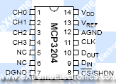
The PIN out of MCP3204 is shown below.
 |
MCP3204 SPI ADC Pin Configuration |
- CH0 : Analog Input Channel 0
- CH1 : Analog Input Channel 1
- CH2 : Analog Input Channel 2
- CH3 : Analog Input Channel 3
- N/C : Not Connected.
- N/C : Not Connected.
- DGND : Digital Ground.
- CS: Chip Select.
- Din : Connected to AVRs MOSI
- Dout : Connected to AVRs MISO
- CLK : Connected to AVRs SCK
- Agnd : Analog Ground
- Vref : Reference Voltage. (Don’t know what is Vref then See: Using the Analog To Digital Converter. )
- Vdd : Positive supply (5v).
SPI Transaction
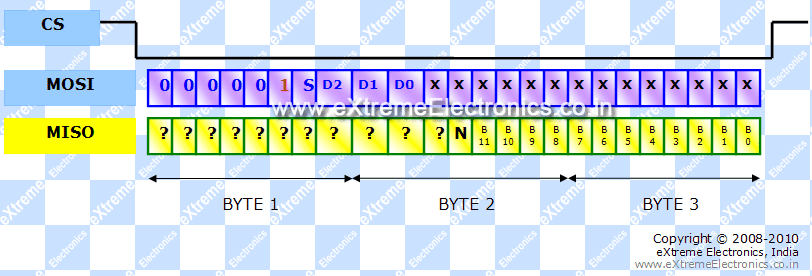
The SPI Packet for one ADC Conversion is made up of 3 bytes. The complete transaction is shown below.
 |
MCP3204 SPI ADC Pin Configuration |
Byte I
In this byte the Master Writes a bit sequence as shown below
‘0’ ‘0’ ‘0’ ‘0’ ‘0’ ‘1’ ‘S’ ‘D2’
Where S is the bit which selects between differential and single ended operation. In our example we need single ended operation and for that this bit must be 1.
Byte II
In this byte MASTER Writes the following sequence
‘D1’ ‘D0’ ‘X’ ‘X’ ‘X’ ‘X’ ‘X ‘X’
Where D2,D1,D0 selects the input channel.
| D2 | D1 | D0 | |
| Channel 0 | 0 |
0 |
0 |
| Channel 1 | 0 |
0 |
1 |
| Channel 2 | 0 |
1 |
0 |
| Channel 3 | 0 |
1 |
1 |
| Channel 4 | 1 |
0 |
0 |
| Channel 5 | 1 |
0 |
1 |
| Channel 6 | 1 |
1 |
0 |
| Channel 7 | 1 |
1 |
1 |
Note: Channel Number 4 to 7 are only available in MCP3208.
And the slave return the following sequence
‘?’ ‘?’ ‘?’ ‘N’ ‘B11’ ‘B10’ ‘B9’ ‘B8’
Where ‘?’ is Unknown bit and may be 0 or 1
‘N’ is Null bit and is always 0
Byte III
In this byte the Master writes a DON’T CARE Byte to slave. You can write any value it does not matters.
In the same time Slave returns bits B7 to B0 of conversion.
So Bit B11 to B0 forms the 12bit result of Analog to Digital Conversion. Following Code Example demonstrate the complete transaction.
/********************************************************************

Requests the ADC to perform conversion and send the result.

Arguments:
      uint8_t ch : Channel Number
      For MCP3204 ch is between 0-3 (Total 4 channels)
      For MCP3208 ch is between 0-7 (Total 8 channels)

Return Value:(TYPE uint16_t, i.e a 16bit unsigned int)
      The digital equivalent of analog input on selected channel.

      Since the ADCs are 12 bit the return value is between
      0-4095 (Including both)

********************************************************************/
uint16_t ReadADCEx(uint8_t ch)
{
   uint8_t byte,data_high,data_low;

   byte=0b00000110;

   if(ch>3)
      byte|=0b00000001;

   CS_LOW();

   SPIWrite(byte);

   byte=ch<<6;

   data_high=SPIWrite(byte);

   data_high&=0b00001111;

   data_low=SPIWrite(0xFF);

   CS_HIGH();

   return ((data_high<<8)|data_low);
}
Example Program
The following program reads the ADC result from MCP3204 and displays it in the LCD module. See the following article from more information about LCD interface routines.
/******************************************************************************


Sample Program to Test "External SPI ADC Interface" libraries. The Simple job
performed by this program is as follows:-

*to connect with external SPI ADC
*ask it to convert a analog value to digital on any channel say channel 0
*read the converted value
*display it in LCD Module


Hardware:
   ATmega32 running @ 16MHz
   FUSE HIGH = 0xC9 LOW=0xFF

   MCP320X Connected to SPI Port

   CS PIN of MCP320X Connected to PD7 (Can be chaned by editing spi.h)

   16x2 LCD Module Connected as
      * RS  -> PD3
      * R/W    -> PD6
      * E      -> PB4

      * D4  -> PB0
      * D5  -> PB1
      * D6  -> PB2
      * D7  -> PB3


                                     NOTICE
                           --------
NO PART OF THIS WORK CAN BE COPIED, DISTRIBUTED OR PUBLISHED WITHOUT A
WRITTEN PERMISSION FROM EXTREME ELECTRONICS INDIA. THE LIBRARY, NOR ANY PART
OF IT CAN BE USED IN COMMERCIAL APPLICATIONS. IT IS INTENDED TO BE USED FOR
HOBBY, LEARNING AND EDUCATIONAL PURPOSE ONLY. IF YOU WANT TO USE THEM IN
COMMERCIAL APPLICATION PLEASE WRITE TO THE AUTHOR.


WRITTEN BY:
AVINASH GUPTA
me@avinashgupta.com

*******************************************************************************/

#include <avr/io.h>

#include "lcd.h"

#include "adc_ex.h"

void main()
{
   //Initialize LCD Module
   LCDInit(LS_ULINE);

   //Initialize External ADC Module
   InitADCEx();

   //A varriable to hold the converted value.

   uint16_t result;

   while(1)
   {
      //Read Channel Number 0
      result=ReadADCEx(0);

      //Display
      LCDWriteStringXY(0,0,"MCP3204 ADC Test");
      LCDWriteStringXY(0,1,"result = ");

      LCDWriteIntXY(9,1,result,5);
   }

}
The complete AVR Studio Project with all relevant support files is available for download. The project composed of the following files
- adc_ex.c : Support file for MCP3204 ADC
- spi.c : Core SPI Communication library. adc_ex.c makes use of these SPI Functions.
- lcd.c : Core LCD Interface Routines.
- SPIADC.c : The main example file making use of functions in above files.
Hardware for Interfacing MCP3204 with AVR ATmega32
Fuse bits must be set so as to enable external crystal and disable JTAG. Example LOW FUSE = FF and HIGH FUSE = C9
After running the demo rotate the POT(RV1) and see the value change in LCD Module. If display is not visible adjust POT(RV2).
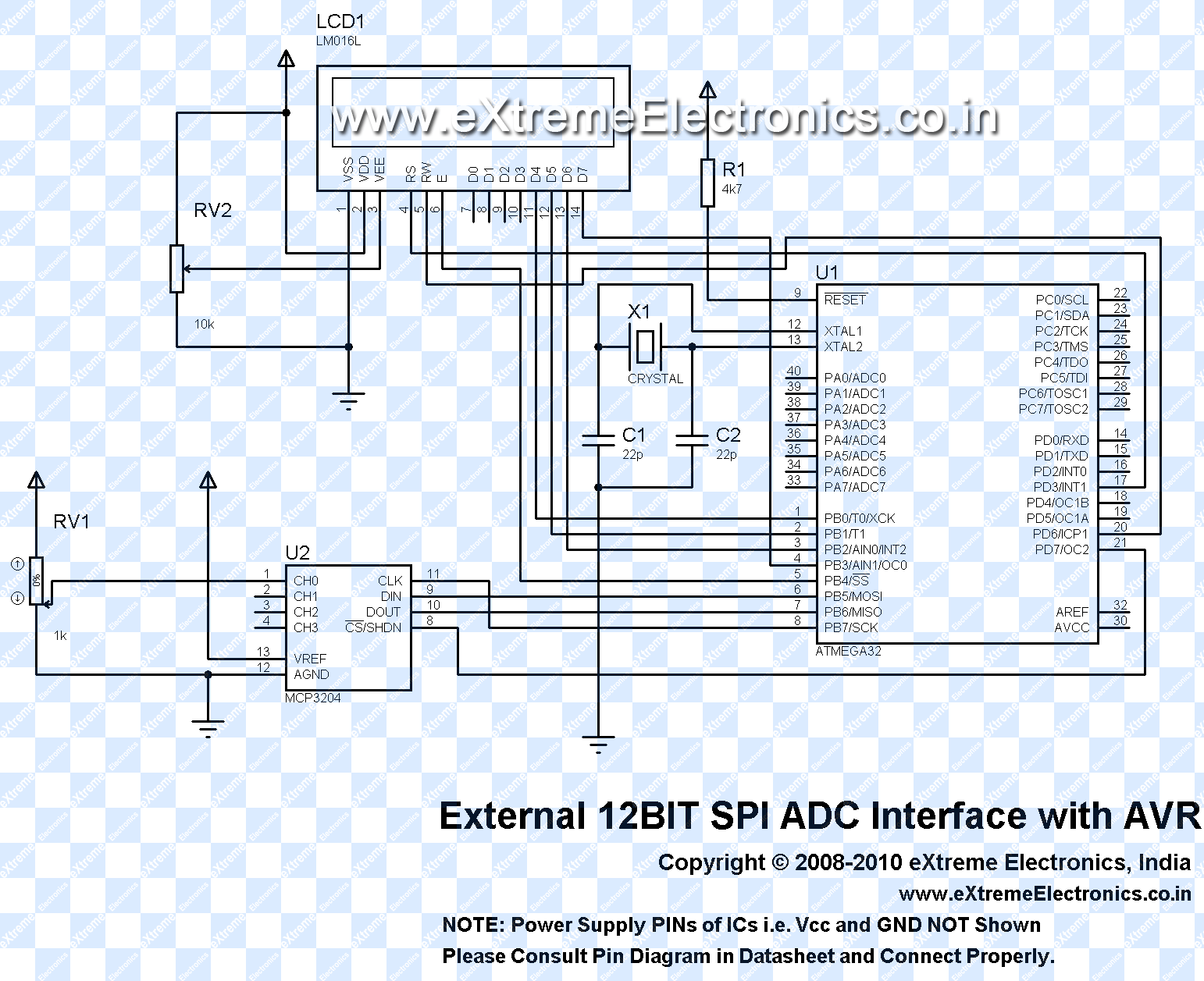 |
Interfacing MCP3204 SPI ADC with AVR ATmega32 |
Downloads
hi can u please upload a c programming to interface mcp3204 with Philips 80c51. its urgent as i require for my project
@Lokesh
Sure why not! Just pay me US$500.
thank u..the amount u asked inspired me to write the program myself and its working really good…
Dear LOKESH,
i written c code for interfacing mcp3202 with p89v51rd2. it is not working properly, give me idea for that please….
Nice post. Found it really helpful.
Can you please explain the purpose of the following lines in the code a bit clearly?? Please sir
byte=ch<<6
data_high&=0b00001111
data_low=SPIWrite(0xFF)
Outstanding tutorial! I have it working using the 10bit version ADC MCP3004 and I can’t seem to work out the scaling of the ADCs. They still go to 4095. Can you provide clue?
This has been profoundly helpful! Keep it up!
please i am new with arduino. i’m using TLC3574 ADC with spi interface and Arduino Uno.
datasheet: http://www.ti.com/product/tlc3574
with the code below the ADC results is either 0 or 1,66
… please help me if you have any idea:
#include
const int dataReadyPin = 6;
const int chipSelectPin = 10;
int result;
// const int chipSelectPin = 10; // SS
void setup() {
SPI_CLOCK_DIV32 ;
SPI.setClockDivider(SPI_CLOCK_DIV128 );
SPI.setDataMode(SPI_MODE1);
pinMode(chipSelectPin, OUTPUT);
pinMode(12, INPUT); //MISO
pinMode(13, OUTPUT); // CLOCK
pinMode(11, OUTPUT); // MOSI
SPI.setBitOrder(MSBFIRST ) ;
SPI.begin();
digitalWrite(chipSelectPin, LOW);
SPI.transfer(0xAE);
SPI.transfer(0x32);
digitalWrite(chipSelectPin, HIGH);
digitalWrite(chipSelectPin, LOW);
SPI.transfer(0x00);
SPI.transfer(0x00); // select Analog input ch0
digitalWrite(chipSelectPin, HIGH);
}
void loop(){
digitalWrite(chipSelectPin, LOW);
result = SPI.transfer(0x10);
result = SPI.transfer(0x00);
delay(1);
digitalWrite(chipSelectPin, HIGH);
digitalWrite(chipSelectPin, LOW);
result = SPI.transfer(0xE0);
result = SPI.transfer(0x00);
digitalWrite(chipSelectPin, HIGH);
delay(100);
}
“The Bset Tutorial Writer Ever”
Than’Q’ Mr Avinash for your extraordinary effort.
Hi, thank you for this tutorial. It was helpful, but i have a question:
If i want to connect more ADC`s and there is just one ss/cs channel on the ATmega32 what do i have to do? Is it possible to do daisy-chainning with all MCP3208?
@Maiara,
Use any other GPIO as SS pin
Sir i have(PSOC) psoc controller devlpomemt kit 3 board …i need your help for interfacing code using spi protocol for interface ADS1278 TO PSOC CONTROLLER PLZ psoc is new for me and i have no idea that how can i interface
Hello guys,
what should be the low and high fuse bit settings for atmega16 running at 16mhz crystal?
Low=0xFF High=C9
Great job great tutorials. was using same code but with atmega1284p . it works nicely in atmega32 but not atmega1284. Since they have same pins for SPI I just swapped the uCs.
Any idea? I will be greatful.
Thank you very much for your tutorial, very informative. My name is Kafou, I am new with spi programming. I am trying to read from ADC 7812 Arduino Leonardo (SPI communication). I only reading 0 from the register, Please help me solve this problem.
Here is the code I have:
#include
const int slaveSelectPin = 10;
void setup() {
Serial.begin(115200);
// set the slaveSelectPin as an output:
pinMode (slaveSelectPin, OUTPUT);
pinMode (MOSI, OUTPUT);
// initialize SPI:
SPI.begin();
}
void loop() {
int result;
// Begin a read or write cycle
digitalWrite(slaveSelectPin, LOW); //Enable the slave
// Send the command to read register 0
SPI.transfer(0);
SPI.transfer(result);
// Now read a byte from the chip. THE VALUE WE SEND MAKES NO DIFFERENCE WHEN READING.
// We just need to generate 8 clock pulses and sample the MISO line to get the data.
// Sending a byte will generate the clock pulses
result = SPI.transfer(0x33);
// Register read operation complete
digitalWrite(slaveSelectPin, HIGH);
Serial.print(“Register 0 contains “);
Serial.println(result);
delay(1000);
}
Hi Avinashg
Hope you are well
Thank you for this tutorial. Has been bery helpful.
Just one thing.
Why is
void SPIInit()
{
//Set up SPI I/O Ports
SPI_DDR|=((1<<MOSI_POS)|(1<<SCK_POS)|(1<<SS_POS));
SPI_PORT|=(1<<SS_POS); This line in the SPInit routine please?
In the diagram Pin PB4 goes to the LCD.
Am I reading this wrong
Hope for your information
Kind regards
James